Showing posts sorted by relevance for query organic mobility. Sort by date Show all posts

Saturday, November 13, 2010

A grand challenge: calculate the charge mobility of a real organic material

Previously I have written several posts about charge transport in organic materials for plastic electronic and photovoltaic devices. This week I looked over two recent articles in Accounts of Chemical Research that discuss progress at the very ambitious task of using computer simulations to calculate/predict properties of real disordered molecular materials beginning with DFT calculations of specific molecules. I was pleased to see that Marcus-Hush electron transfer theory plays a central role in both papers,

Electronic Properties of Disordered Organic Semiconductors via QM/MM Simulations (from the group of Troy Van Voorhis at MIT). 

Modeling Charge Transport in Organic Photovoltaic Materials (from Jenny Nelson's group at Imperial College London).

I have several questions and concerns about the latter paper.

The authors do a rather sophisticated simulation of a time of flight experiment where they put a charge accumulation on one side of the sample, apply an electric field, and measure
the average charge velocity, and extract the mobility. Intermolecular hopping rates are given by Marcus-Hush theory with parameters extracted from DFT calculations.

1. Is this the most efficient and reliable way to calculate mobility?
Generally in solid state physics one uses the fluctuation-dissipation relation. In this case Einstein's relation the mobility can be obtained from the diffusion constant. The diffusion constant is just the intermolecular hopping rate times the square of the intermolecular distance.

2. The mobility computed depends on the thickness of the sample.

3. How was the calculation benchmarked? Does this method give reliable
results for simpler systems, e.g., a naphthalene crystal?

4. The abstract makes some very strong claims,
"these computational methods simulate experimental mobilities within an order of magnitude at high electric fields. We ... reproduce the relative values of electron and hole mobility in a conjugated small molecule... We can reproduce the trends in mobility wiht molecular weight ... we quantitatively reproduce...On the basis of these results, we conclude that all of the necessary building blocks are in place for the predictive simulation of charge transport in macromolecular electronic materials and that such methods can be used as a tool toward the future rational design of functional organic electronic materials."


But when I look at the graph above it looks to me that the method often disagrees with experiment by more than an order of magnitude and fails to capture any electric field dependence. I could not find any discussion of temperature dependence.

Monday, November 1, 2010

Dielectric relaxation in organic electronic devices

A recent post mentioned the paper Low-k insulators as the choice of dielectrics in Organic Field-Effect Transistors [by Veres et al.], in the context of the sticky point of how to determine the relative importance of disorder and polaronic effects in molecular conducting materials used in semiconductor type devices. 

A major point of the paper is something different: how the mobility measured by time of flight (TOF) measurements is distinctly different [it has a larger magnitude and smaller activation energy] from in FETs, and that the mobility in FETs can decrease significantly with increasing the dielectric constant of the material used in the gate insulator material.

The paper discusses extensively how this may be associated with different kinds of disorder at the interface [which was followed by a theoretical paper in J. Chem. Phys. by Richards, Bird, and Sirringhaus]. It is not clear to me that invoking disorder is necessary to explain the gate dielectric dependence sure this is necessary. The reorganisation energy (polaron binding energy) associated with charge transfer between neighbouring molecules varies significantly with the dielectric constant of the surrounding medium. [Reminder: the activation energy for the mobility is 1/4 of this reorganisation energy].

For molecules close to the interface between the gate insulator and organic semiconductor, this reorganisation energy will decrease with a decrease in the dielectric constant of the insulator. Furthermore, if the organic semiconductor has a dielectric constant less than the gate dielectric, the reorganisation energy associated with a bulk measurement such as TOF will be less than a FET measurement which measures charge transport close to the interface.

Indeed the observed dependence of the FET mobility on the gate dielectric constant is observed explained within the framework of small polaron theory in a 2005 Nature Materials paper, Tunable Frohlich polarons in organic single-crystal transistors [see Figure above].

Friday, February 19, 2010

Is "organic semiconductors" a misnomer?

A wide range of organic molecular materials such as pentacene and polythiophene are attracting considerable interest because of the prospect of "plastic electronics". They can be used to fabricate devices such as light emitting diodes, photovoltaic cells, and field effect transistors, which are traditionally made with inorganic semiconductor materials such as silicon and gallium arsenide. Consequently, these organic materials are often referred to as organic semiconductors. This may seem reasonable because:
  • they have a conductivity that is activated in temperature
  • there is an energy gap of several eV to the lowest optically excited state
  • they can be used to make "semi-conductor type" devices
On the other hand, they have properties that are significantly different from inorganic semiconductor materials. These all relate to the fact that electronic states tend to be localised on single molecules whereas in inorganic semiconductors one can have states which are delocalised over many atoms.
  • they do not have well-defined conduction and valence bands (e.g., their mobility is almost always much less than that required for band transport) [just because you can calculate something does not mean it exists!]
  • they have a mobility that is thermally activated
  • energy gaps associated with optical absorption and conduction are significantly different
  • electronic correlations significantly modify the ordering of electronic states (e.g. there is a large gap between singlet and triplet excited states)
Because there is no band transport one cannot define a scattering time and one should not talk about "band bending" near an interface.

I think that referring to these materials as organic semiconductors has led a lot of confusion and debatable reasoning in the literature. I think "organic electronic materials" or "organic photonic materials" is much more appropriate.

Tuesday, September 4, 2012

Signatures of "band-like" transport in organic electronic materials

I used to regularly write posts about charge transport in organic electronic materials. Some of these generated lively discussion in the comments section.

This morning I read an interesting paper Band-Like Electron Transport in Organic Transistors and Implication of the Molecular Structure for Performance Optimization
by Nikolas Minder, Shimpei Ono, Zhihua Chen, Antonio Facchetti, Alberto Morpurgo

They correctly distinguish "band-like" transport where a charge carrier is delocalised over just a few molecules from true band transport where it is delocalised over a large number of molecules [or unit cells in a crystalline semiconductor such as silicon].

They claim that a signature of band-like transport is the common observation of a mobility that decreases with increasing temperature and a Hall effect signal. I agree with the former but am confused about the latter. I thought for incoherent polaron transport one could still have a Hall effect, as discussed in a classic paper by Friedman and Holstein. 

The authors overlook the fact that a signature of band-like transport is that the mobility should be larger than e a^2/hbar ~ 1 cm^2/Vsec. Ignorance of this old and important result seems to be common in the field.

Previously, I pointed out that comparing the relative magnitudes of the energy gaps respectively associated with mobility, optical conductivity, and thermopower is a nice way to distinguish coherent from incoherent transport.

Monday, July 20, 2009

Electron vs. hole transport in organic materials

A general observation is that the mobility for electron transport in organic materials used in electronic and photonic devices can be orders of magnitude smaller than the mobility for hole transport. A rough explanation for this is given in a useful review by Bredas et al. The figure below is the basis for the discussion of how for a pair of adjacent molecules the splitting of HOMO's is larger than that of LUMO's.


This splitting is proportional to the matrix element (t in a Huckel model) between orbitals on different molecules. This is larger for the HOMO's because the wavefunction has fewer nodes than the LUMO does and so the intermolecular overlap is less.
The mobility is proportional to t^2 (see the review by Horowitz) and so is much smaller for electron than hole transport.

However, this is not the end of the story since one also needs to consider effects such as whether impurities in an actual material are more effective at trapping charge carriers for electrons or for holes. Such issues are discussed in this Nature paper concerning n-type organic FET's.

Saturday, February 20, 2010

Proton conduction in organic FETs?

This title is deliberately provocative. It is keeping with the notion of multiple alternative hypotheses. I note the following concerning organic Field Effect Transistors
  • The mobility of protons in water is 3 x 10⁻³ cm^2/Vs.
  • This is larger than the hole mobility in many OFETs.
  • Fabrication of many OFETs involves treatment with acids at some stage.
  • Gate dielectric surface treatments significantly affect device performance, as described in this review.
So can someone rule out the following hypothesis?
In some organic FETs there is actually a contribution to the current from protons (rather than holes) moving in the interface between the organic "semiconductor" and the gate dielectric.

Perhaps a systematic study of OFET performance as a function of humidity?

Friday, January 29, 2010

Beware of curve fitting

In a comment on a previous post about charge transport in organic materials Doug Natelson brought to my attention a recent preprint. It is a really nice paper and is a cautionary tale about drawing conclusions from curve fitting.

In a Nature Materials paper last year, Alan Heeger's group at UCSB considered the electric field and temperature dependence of the current in an organic field effect transistor. They fitted the observed dependence to that for a theory which describes slightly dirty long one dimensional conducting wires with strong electronic correlations (Tomonaga-Luttinger liquid theory). This theory gives a good description of charge transport in single carbon nanotubes. However, it is not clear if there is a physical reason to expect the TLL theory to be relevant to "dirty" crystals of small organic molecules.

However, Worne, Anthony, and Natelson show that for their data on similar devices the curve fitting to the TLL theory is problematic. In particular, the apparent "scaling collapse" is fortuitous. They state:

decreasing T moves subsequent temperature data sets up and to the right on the graph, even if the data themselves do not change with temperature at all. In fact, any weakly temperature dependent dataset that resembles a power-law can be made to fit onto a single line if plotted in this way with an appropriate choice of α. Data collapse with this plotting procedure is not sufficient to demonstrate TLL physics.

There is another reason why I am skeptical about any claim of "metalllic" behavior in these systems. Their mobility is much less than than the "minimum mobility"of 1 cm^2/Vsec that is necessary for the coherent transport associated with delocalised electrons and band structure.

Friday, October 29, 2010

Deconstructing charge transport in organic semiconductors

A key question about charge transport in organic molecular materials is:

What is the relative importance of disorder and dielectric relaxation [small polarons = Marcus-Hush theory] in determining the charge mobility?

There is a nice clear and succinct review article in Chemical Reviews from 2007 by Coropceanu et al.

The view that disorder is dominant has been advocated by Bassler and collaborators, in
terms of a Gaussian density of states. This leads to a  mobility with the temperature dependence

[I have not seen an analytical derivation, this seems to be based on curved fitting to the results of Monte Carlo simulations].
This is in contrast, to an activated form.


Aside: Coropceanu et al. claim "there is no full theoretical justification for such an Arrhenius like expression". I am mystified by this claim. Small polaron theory [and equivalently Marcus-Hush theory, together with the fluctuation-dissipation theorem] give such a form. Indeed, in the review article they later give such expressions.
But, that is not my main point.

It is also pointed out that distinguishing between these two models is difficult
with experimental data from a limited temperature range.
This can be seen clearly in the Figure below taken from a 2003 paper Low-k insulators as the choice of dielectrics in Organic Field-Effect Transistors


Hence, just because one can fit the data to one of the models one should NOT conclude that model is correct. Unfortunately, this is often forgotten...

Presumably measurements down to 1 K may help distinguish the two models, although apparently these devices can malfunction at lower temperature.

I have more to say about this data, and what it may say about the charge transport mechanism,  but will leave that for another day...

Thursday, May 28, 2009

A simple transport criterion for the absence of energy bands

A lot of papers on materials for organic electronics and photonics will discuss transport and optical properties in terms of conduction and valence bands, concepts that are valid and useful for inorganic crystalline semiconductors.

But, I do not think such bands exist for most of these materials. This can be seen from the magnitude of the transport mobility. These notes show a simple self-consistency argument which shows that if band transport is meaningful (i.e., one can talk about electrons with a definite wavevector and which are occasionally scattered) then the mobility must be much larger than about
e a^2/hbar ~1 cm^2/Vsec.

I derived this result over a year ago but then discovered this appears to have been well known back in the 70's, and seems to have been forgotten.

For example, the result is clearly stated:

in equation (24) of a 1963 paper by Glarum.

in equation (224) on page 24, of a classic 1971 review of Metallic Oxides by John Goodenough

page 346, of the second edition of Pope and Svenberg's Electronic processes in organic crystals and polymers.

Thursday, July 1, 2010

Charge transport in organic photovoltaic materials

Today I am chairing a session on charge transport at an I2CAM Exploratory Workshop, Complex Interactions and Mechanisms in Organic Photovoltaics being held here at UQ.
I have written quite a few posts on this topic before. I believe some of the key questions concerning charge transport in molecular materials are:
  • What is the mechanism of charge transport?
  • What is the origin of the observed electric field dependent mobility?
  • What determines the relative magnitude of electron and hole mobilities?
  • How does mobility depend on the intermolecular separation and relative orientation?
  • Would thermopower measurements be helpful in determining the charge transport mechanism?

Friday, August 7, 2009

Charge mobility in dendrimers


This post was stimulated by a talk at last weeks COPE meeting and looking at this 2001 Phys. Rev. B paper from the groups of Samuel and Burn.


In the attached rough notes I try to provide a framework to answer questions such as:

What determines the charge mobility in an array of these systems? How can it be maximised?

What is the relative importance of the conjugated and non-conjugated components of the dendrimer?

I take it the non-conjugated surface groups are required to make these systems soluble.
It seems that the mobility falls off exponentially fast with the length of the non-conjugated molecules at the surface. (roughly an order of magnitude for every carbon in the chain?)

Understanding the notes may be made easier by ready some of my earlier organic electronics posts, especially this one on Hush-Marcus electron transfer theory.

Monday, September 30, 2013

Signatures of charge fluctuation mediated superconductivity

Superconducting organic charge transfer salts are diverse. One class that has attracted considerable attention are the kappa-ET and dmit families that can be described by a Hubbard model on the anisotropic triangular lattice at half filling. Superconductivity emerges out of the parent Mott insulating state. The half filling arises because the molecules occur in pairs [dimers] within the crystal structure. Each dimer corresponds to a site in the lattice for the Hubbard model.

In a second class of materials the molecules are not dimerised and the resulting electronic bands are one-quarter filled with holes. Each site in the relevant lattice is a single molecule. The superconductivity emerges out of a charge-ordered [Wigner-Mott] insulator. The simplest possible effective Hamiltonian is an extended Hubbard model at one-quarter filling on a square lattice. In a 2001 PRL Jaime Merino and I showed how superconductivity could occur in these materials as a result of charge fluctuations associated with proximity to charge ordering.

Is this really true? How might you see the charge fluctuations and/or charge order? In crystals where each lattice site is a single atom [e.g. a transition metal ion] one might use inelastic x-ray scattering. However, in molecular systems one has more degrees of freedom since each lattice "site" consists of a large organic molecule. The intramolecular vibrations provide a nice knob to see the local charge density and its fluctuations. Specifically, the frequency and infra-red intensity of an antisymmetric C=C stretch on the BEDT-TTF molecule is particularly sensitive to the charge on the molecule, as parameterised here by Alberto Girlando.

The schematic phase diagram below places two different compounds beta''-M and beta''-SC. The former has a metallic ground state and the latter superconducting and is closer to the charge ordered state.

Bandwidth Tuning Triggers Interplay of Charge Order and Superconductivity in Two-Dimensional Organic Materials
S. Kaiser, M. Dressel, Y. Sun, A. Greco, J.A. Schlueter, G.L. Gard, and N. Drichko

One can contrast the infra-red vibrational spectra of these two compounds. In the lower right of the figure below one sees two sharp vibrational features corresponding to two distinct charge states of the molecule in the beta''-SC compound. At higher temperatures there are large charge fluctuations between these two charge states. In the beta''-M compound one does not see the charge order, just charge fluctuations.

The figure is taken from
Spectroscopic characterization of charge order fluctuations in BEDT-TTF metals and superconductors
A. Girlando, M. Masino, S. Kaiser, Y. Sun, N. Drichko, M. Dressel, H. Mori

The authors fit the spectra to a "jumping two-state" model of Kubo [described in a1969 Adv. Chem. Phys. review], which involves a hopping [or exchange] rate, about 10-30 cm-1 between the two charge states.

There are several interesting issues this work raises and some opportunities for future work.

1. What exactly does the hopping rate [exchange frequency] extracted from the experiment represent physically? How is it (not) related to charge mobility or the diffusion constant associated with charge fluctuations with wave vector (pi,pi)?

2. The theory predicts d_xy superconductivity. This means there should be nodes in the energy gap? are they present? There is some evidence from one penetration depth measurement.

3. Both materials should be bad metals at temperatures of the order of tens of Kelvin. The resistivity is certainly large and a Drude peak is only seen at low temperatures. It would be nice to see some thermopower measurements since they are particularly sensitive to a Fermi liquid bad metal crossover.  Theoretical calculations [using the Finite Temperature Lanczos Method] do predict a bad metal close to the charge ordered phase.

4. The title of this post may be an over-simplication. A weak coupling analysis may reveal it is not so easy to separate out spin and charge fluctuations.

I thank Alberto Girlando and Matteo Masino for explaining their work to me.

Thursday, August 14, 2014

Scale of the Nernst effect in a bad metal

A science fiction fantasy is that we should be able to make "materials by design" that have any physical property (density, thermal conductivity, hardness, thermoelectric figure of merit, heat capacity...)  that we desire. However, it seems that there are certain physical constraints that determine the overall scale of many physical properties.

I find it helpful to have a feel for typical orders of magnitude. What is particularly interesting is that sometimes these magnitudes are related to fundamental constants [electronic charge (e), Boltzmann's constant (k_B), Planck's constant (hbar)] and basic length scales such as the lattice constant a of a crystal.

Here are three scales I have emphasised before

Resistivity ~ hbar a / e^2 ~ 100 microohm-cm  which is associated with the Mott-Ioffe-Regel limit.

Thermoelectric power,  S ~ k_B/e ~ 86 microvolt/K

Mobility, mu ~ e a^2/ hbar ~ 1 cm^2 V/sec

One can find these scales by dimensional analysis or by doing things like looking a formulas from transport theory and (assuming a bad metal) setting the mean-free path comparable to the lattice constant. One can debate whether one uses hbar or h, but for little purpose.

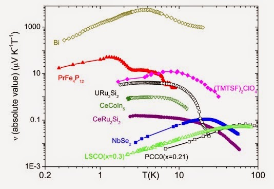
How about the Nernst signal, nu?

nu ~ k_B a^2 / hbar ~ 0.01 microV/KT

A few minor notes.

1. One can get this scale from the above expressions for S and mu if one uses the observation that in some strongly correlated materials
nu ~ S * Hall mobility.

2. One Volt/Tesla = m^2/sec  [One can see this easily from F = q(E + vxB)].

3. Given that the Nernst effect involves charge transport I find it surprising that the electronic charge does not appear.

The figure below, taken from a nice review by Behnia, shows that this is the right scale for bad metals such as cuprates, and heavy fermions above the coherence temperature.

One also sees this scale in recent DMFT calculations for a doped Hubbard model (see Figure 2d in this PRL ) and recent measurements (see Figure 4) on organic charge transfer salts.

Tuesday, March 30, 2010

An equation you should know

Next month I am going to India to speak at a School and Conference on “Emergent Properties and Novel Behavior at the Nanoscale” organised by I2CAM and the Jawaharlal Nehru Centre for Advanced Scientific Research (JNCASR) in Bangalore.

In the school I will give a one hour long lecture. Here is the abstract I have submitted. Any feedback welcome. Some related material is discussed in this talk I gave last year in the Black Forest.

Quantum design principles for functional electronic materials

In a complex material how does one optimise the quantum efficiency of the transition
between two different quantum states when there are many alternative transitions available to a system?

Regardless of whether or not it is explicitly stated this is the question which is at the heart of a wide range of research. Prominent examples include understanding biomolecular function, designing organic photovoltaic cells, and catalysis.

I will discuss how this optimisation problem involves a subtle interplay between quantum coherence and decoherence induced by the system environment. The essential physics involved can be understood in terms of the spin-boson model which describes two quantum states which are coupled to one another with an environment which is modelled by a collection of an infinite number of harmonic oscillators.

Qualitatively different dynamics occurs depending on the relative magnitude of the key energy and time scales in the problem: the thermal energy, energy difference between the two states (epsilon), the coupling of the two states (and the associated Rabi frequency), the reorganisation energy of the environment, and the typical relaxation time of the environment.

Perhaps it is not appreciated enough that for most systems of interest all of these energy scales are well-characterised.

The incoherent "classical" regime of the spin-boson model gives a simple expression for the transition rate which is the same as the Marcus-Hush expression for the electron-transfer rate. I consider this is one of the most important equations in chemical physics and particularly for the understanding and design of functional materials.

I will discuss several important applications of this equation.

1) A design principle:
The rate is a maximum for a specific non-zero value of the coupling to the environment where epsilon equals the reorganisation energy.

2) The temperature dependence of the charge mobility in molecular materials.
[This is the same expression as given by small polaron theory].

3) Forster resonant energy transfer between chromophores.

Thursday, April 21, 2011

Goldilocks on superconductivity

Manifesto for a higher Tc by Dimitri Basov and Andrey Chubukov is an interesting Perspective in Nature Physics. It contains a nice comparison of the new "iron pnictide" superconductors with the cuprates.

They identify three key questions:
(1) Do all high-Tc materials superconduct for the same reason? 
(2) Are the rather anomalous normal-state properties of exotic superconductors a necessary prerequisite for high-Tc superconductivity? 
(3) Is there a generic route to increase Tc
They claim that the answer to (1) is yes, exchange of spin fluctuations associated with nesting of different parts of the Fermi surfaces. I am not sure if the majority of people would agree with them on this point.

A few things the Basov and Chubukov also highlight
  • The reduction of the kinetic energy by strong correlations deduced from the optical conductivity is a convenient way to characterise the strength of interactions. They claim a 50-70% reduction is optimum for a high Tc. There is a balance ["just right" as found by Goldilocks!]. Stronger interactions increase the pairing interaction but also decrease the mobility of the Cooper pairs.
  • The connection between the superfluid density and the loss of low energy spectral weight in the optical conductivity. [Strong dissipation reflected in the Homes scaling where the superfluid density is proportional to the product of Tc and the intralayer dc conductivity.]
In passing, I note that the reduction of the kinetic energy has been measured and discussed for a family of superconducting organic charge transfer salts in this PRL. [Although for idiosyncratic historical/experimental reasons it is plotted as the effective number of charge carriers].

I thank Ben Powell for bringing the paper to my attention.

Sunday, July 4, 2010

OPV cell efficiency is an emergent property

As discussed in a previous post, the efficiency of organic photovoltaic (OPV) cells appears to be largely determined by solid state (and thus collective) effects such as aggregation, sample morphology, and disorder. A striking example of this is that the efficiency of a cell can be improved significantly by annealing the thin film (i.e., just taking the film and slowly heating and then cooling it). Hence, efficiency is an emergent property and reductionist theoretical approaches that focus on the properties of isolated constituent molecules have debatable value.

At the I2CAM workshop this past week the most disappointing presentation was that from the Harvard clean energy project, led by Alan Aspuru-Gizek . This very ambitious project aims to using the world wide grid of computers (including your own PC) to run quantum chemistry codes to calculate properties of hundreds of thousands of molecules to screen them as candidates for use in OPVs. However, it must be stressed that almost all of these calculations will be on small single and isolated molecules in the gas phase.

It was claimed that one could screen for high charge mobility materials by looking at delocalisation of frontier orbitals and the reorganisation energy associated with ionisation. However, the particularly relevant quantity is the reorganisation energy of the environment of the molecule.

The speaker claimed something like "we are our own harshest critics" and listed possible weaknesses of the project. These were most concerned with whether approaches based on density functional theory (DFT) are adequate for calculating the relevant properties of these molecules. (Many people would say they are not). However, I contend that even if one could calculate exactly the properties of single molecules in the gas phase one would be a long way from being about to determine which molecules will be the best candidates for OPVs.

I asked for a specific example of where such a computational approach has been successful for any area of science and technology. It was stated that drug companies do this all the time when screening. However, I contend the physics and chemistry of that problem is much simpler and more well defined. One knows a specific active site of a protein that ones want to find a small molecule to bind to the hinder the activity at that site. This is a ground state and very local property. In contrast, for photovoltaics excited states, dynamics, and collective effects are involved, and the relevant large scale structures are not well defined. Exactly how the properties of OPVs are related to the properties of the constituent molecules is so poorly understood I am skeptical that a brute force computational approach is going to lead to much progress.

Saturday, January 23, 2010

Searching for a unified description of charge transport in molecular materials


Chemical Reviews just released a special issue on Materials for Electronics. There is a helpful article by David Weiss and Martin Abkowitz, Advances in Organic Photoconductor Technology. They note:
The story of the development of electrophotography is an object lesson in the connections between technology development, product development, and scientific understanding.
I found Section 6.1: Charge transport models particularly useful. It contains a critical and succinct discussion of the challenge of coming up with a model which can describe the dependence of the charge mobility on intermolecular separation, temperature, and electric field of a wide class of materials.

The conclusion is "questions remain and a complete description of charge transport in (molecularly doped polymers) MDPs remains elusive"

Lecture on degenerate Fermi gases at low temperatures

Here are the slides for an undergraduate lecture I gave today. The slides also include the derivations I gave by hand on the document viewe...